Our Markets

End-to-end semiconductor infrastructure solutions for foundries, OSAT & ATMP facilities, and R&D laboratories across India.

Advanced technology facilities

Semicon Fab Technologies delivers specialised EPCM and EPCC solutions across the semiconductor value chain — from ultra-clean foundry environments to packaging, testing, and research infrastructure.

Semiconductor foundry solutions
Market 01

Semiconductor Foundry Solutions

Semiconductor foundries are among the most complex engineering environments in the world, requiring extreme precision, advanced infrastructure, and highly controlled cleanroom ecosystems. Semicon Fab Technologies is one of the first Indian companies delivering complete end-to-end semiconductor cleanroom and foundry solutions through strong international collaborations and global technical partnerships.

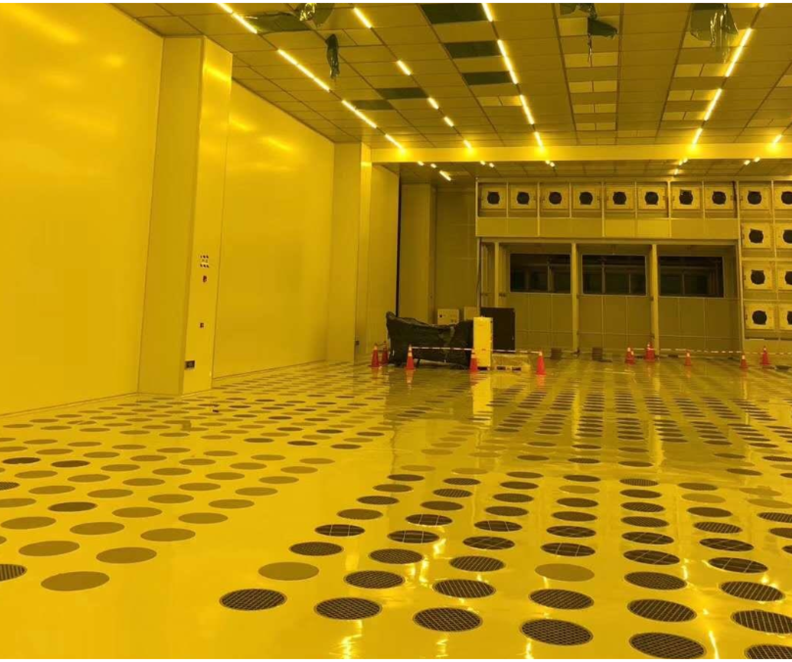
We provide comprehensive EPCM and EPCC solutions covering the entire project lifecycle — from feasibility studies and site selection to detailed design, engineering, construction, commissioning, and validation. Our expertise includes advanced Class 1 and Class 2 ballroom-type cleanroom design and execution for semiconductor manufacturing facilities.

With deep technical knowledge in semiconductor infrastructure, process utilities, HVAC systems, contamination control, and cleanroom validation, Semicon Fab Technologies stands at the forefront of India’s semiconductor infrastructure development.

Our Core Services

  • Feasibility Study & Master Planning
  • Site Selection & Infrastructure Assessment
  • Semiconductor Cleanroom Design (Class 1 to Class 1000)
  • Ballroom-Type Fab Engineering
  • HVAC & Contamination Control Systems
  • Process Utility Engineering
  • EPCM & EPCC Project Execution
  • Testing, Commissioning & Validation
  • International Technical Collaboration & Support

Why Semicon Fab Technologies

  • End-to-end semiconductor fab infrastructure solutions
  • Expertise in ultra-clean semiconductor environments
  • International technology partnerships
  • Advanced engineering and validation capability
  • Strong execution team for complex industrial projects
  • One of India’s emerging leaders in semiconductor cleanroom solutions

At Semicon Fab Technologies, we are committed to building world-class semiconductor manufacturing infrastructure that supports the future of India’s semiconductor ecosystem.

OSAT and ATMP facility solutions
Market 02

OSAT & ATMP Facility Solutions

The OSAT (Outsourced Semiconductor Assembly and Testing) and ATMP (Assembly, Testing, Marking, and Packaging) sectors are among the fastest-growing opportunities in India’s semiconductor ecosystem. With strong logistics connectivity, a rapidly expanding electronics market, and cost-effective skilled manpower, India is strategically positioned to become a global hub for semiconductor packaging and testing facilities.

Semicon Fab Technologies delivers specialised infrastructure solutions for OSAT and ATMP facilities with complete EPCM and EPCC capabilities tailored for semiconductor packaging and testing environments.

We provide end-to-end engineering solutions for advanced Class 10 to Class 100K cleanroom facilities designed specifically for semiconductor assembly, testing, marking, and packaging operations. Our solutions are engineered to meet the stringent environmental and process requirements of modern semiconductor manufacturing.

Our OSAT & ATMP Solutions

Semiconductor Cleanroom Solutions

  • Class 10 to Class 100K cleanroom design and construction
  • Ballroom-type and modular cleanroom concepts
  • Contamination-controlled manufacturing environments
  • Temperature and humidity-controlled process areas
  • ESD-safe cleanroom infrastructure

Process Utility Engineering

  • Vacuum Systems
  • DI Water Systems
  • CDA (Clean Dry Air) Systems
  • Process Exhaust & Scrubber Systems
  • Nitrogen & Specialty Gas Integration
  • HVAC and Airflow Management

EPCM & EPCC Services

  • Feasibility Study & Facility Planning
  • Site Evaluation & Infrastructure Assessment
  • Engineering Design & Process Integration
  • Construction Management
  • Testing, Commissioning & Validation
  • Utility Hook-up & Tool Installation Support

Why India for OSAT & ATMP

  • Cost-effective skilled workforce
  • Strong domestic electronics manufacturing growth
  • Strategic logistics and port connectivity
  • Government support for semiconductor manufacturing
  • Growing semiconductor supply chain ecosystem

Why Semicon Fab Technologies

  • Specialized semiconductor cleanroom expertise
  • Tailor-made utility solutions for ATMP operations
  • International engineering collaboration
  • Strong experience in contamination control systems
  • Complete infrastructure integration capability
  • Reliable EPCM and EPCC execution model

Semicon Fab Technologies is committed to supporting India’s semiconductor growth by delivering advanced, scalable, and reliable OSAT and ATMP infrastructure solutions aligned with global semiconductor manufacturing standards.

Semiconductor R&D and Centre of Excellence
Market 03

Semiconductor R&D Labs & Centre of Excellence (CoE) Solutions

Semicon Fab Technologies is one of India’s emerging specialists in developing Semiconductor R&D Laboratories and Centre of Excellence (CoE) facilities for academic institutions, research organizations, innovation hubs, and semiconductor training centers.

We provide complete end-to-end solutions for semiconductor research, training, prototyping, and advanced technology development infrastructure. Our expertise covers both infrastructure and equipment integration, enabling institutions to establish world-class semiconductor research and learning environments through a single solution platform.

Complete CoE & R&D Infrastructure Solutions

Semicon Fab Technologies delivers turnkey EPCM and EPCC solutions for:

  • Semiconductor Research Laboratories
  • Centre of Excellence (CoE) Facilities
  • Semiconductor Training Centres
  • University Research Labs
  • Innovation & Prototype Development Labs
  • Semiconductor Process Development Facilities

Our Expertise

Semiconductor Cleanroom Infrastructure

  • Class 10 to Class 100K cleanroom solutions
  • Modular and ballroom-type cleanroom concepts
  • Temperature & humidity-controlled environments
  • ESD-safe laboratory infrastructure
  • Advanced contamination control systems

Process Utility Solutions

  • DI Water Systems
  • Vacuum Systems
  • CDA (Clean Dry Air) Systems
  • Process Exhaust Systems
  • Specialty Gas Systems
  • HVAC & Environmental Control Systems

Equipment & Lab Integration

  • Semiconductor laboratory equipment planning
  • Utility integration for process tools
  • Research equipment installation support
  • Customized infrastructure for training and R&D applications
  • Tool room and process lab setup support

End-to-End Project Execution

  • Feasibility Study & Planning
  • Facility Design & Engineering
  • Infrastructure Development
  • Cleanroom Construction
  • Process Utility Installation
  • Equipment Integration Support
  • Testing, Commissioning & Validation

Single Platform Solution Provider

Semicon Fab Technologies offers academia, universities, research institutes, and innovation centers a single platform for complete semiconductor laboratory and CoE development. Our integrated approach reduces project complexity while ensuring reliable, scalable, and future-ready semiconductor research infrastructure.

Why Choose Semicon Fab Technologies

  • Specialized semiconductor infrastructure expertise
  • End-to-end turnkey execution capability
  • International engineering collaboration
  • Customized solutions for training and research applications
  • Advanced cleanroom and utility engineering
  • Strong focus on innovation-driven semiconductor development

We are committed to supporting India’s semiconductor ecosystem by enabling world-class research, innovation, skill development, and advanced semiconductor technology training infrastructure.

Ready to discuss your semiconductor facility project?

Contact Us